The Development of
the TSI Speech+
Speaking Calculator

One day early in 2015 a very interesting email was received from Grant Still Shatto, II, saying:
"I was pleasantly surprised to discover your Vintage Calulators web museum page, and to see the TSI Speech+ talking calculator.
In 1977, I worked for an integrated circuit design company called Silicon Systems, Inc., in Tustin, California. Telesensory Systems came to us and asked us to develop the speech chip for them, and I was the lead mask designer on the project. It was an exciting project, because it was so different than other projects. It actually performed a "real-life" function you could relate to as compared with the disk drive chips we were typically doing at the time.
When the chips came back from the fab and the engineer plugged it in and it made the first "word" sound, it was the most exhilarating moment you could imagine. It was like the NASA control room when the moon lander touched down! High-fives all around.
Our company was given several of the calculator demo units, and I showed one around to all of my friends to impress them. That unit was then loaned to Johnny Carson for one of his "new gadget" segments he did on his Tonight Show. I eagerly watched that segment and was thrilled as his eyes lit up and twinkled with delight at this amazing new technology. He played with it for several minutes, clearly fascinated by it. Afterward, he refused to return it!
So that's my claim to fame!"
The TSI Speech+ calculator itself has a claim to fame since when it was launched in 1976 it was the first speaking calculator, being designed for the visually impaired, and one of the first consumer products with speech synthesis.
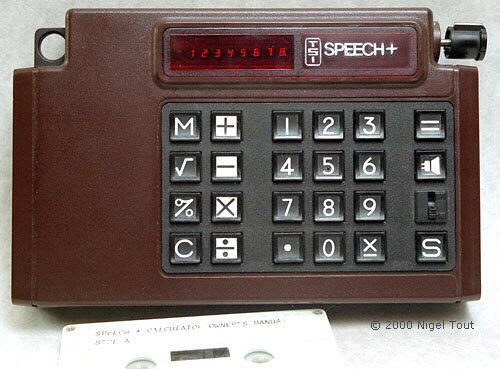
A production TSI Speech+ calculator (serial number S1A 005262) together with the operating instructions on cassette tape.
Grant kindly offered to provide a contact to Ed Bernard who worked for Silicon Systems, Inc., the company which developed and supplied the S14001A speech synthesis chip. Ed was the design engineer for the S14001A and has kindly provided the following information from his notes and his memory of his work on it in the mid 1970s:
"I'll focus on the project aspects of the S14001A development. Silicon Systems, Inc., referred here as SSi, was approached in March of 1975 by Telesensory Systems, Inc, referred to as TSi. TSI were developing a talking calculator for the blind and needed an integrated implementation of Dr. Forrest S. Mozer's algorithm for speech synthesis. It was quite apparent that there was a good fit between their needs and SSi's capabilities. A cost for design, prototype samples and follow on parts cost was proposed and design work began in late March or early April. By late July layout was complete and masks were ordered. Wafers were supplied by Frontier, Inc. of Costa Mesa, CA. First silicon arrived in late September and the design "worked first time". There was considerable clock noise on the "analog" output, but this was not a show stopper as the sound system needed clock noise filtering in any event. Production parts were supplied late in 1975 or early 1976.
The chip was designed using p-channel, depletion load, 2-phase dynamic logic, running at 13KHz. It contained about 1500 transistors and was about 150mil [0.150in] on a side. The process used 6 total masks (p+, gate, implant, contact, metal and pasivation). Minimum line widths for p+ and metal were 0.0003in. There was nothing high tech about the silicon. What was a bit advanced was an on board 4 bit D/A. This was implemented in a full parallel approach using 4 capacitors of 16,8,4 and 2 picofarad. This is primitive compared to the time sequential approach using a single capacitor developed around that time at Berkeley, but it fit well into the overall timing of the chip.
The high tech part of the Speech+ calculator was Dr. Forrest S. Mozer's algorithm, which fit the data required for the 24 word vocabulary into a 4 kilobyte ROM. More on this in the follow on email. An example of careful data use was the change sign key on calculator. Note it is marked with an X/-. The calculator already had an 'X' key, spoken as "Times", and a '-' key, spoken as minus, so the 'X/-' key was spoken as "times minus". Given the data layout of the ROM this "times minus" speech only cost an additional 2 bytes. 4K ROM sounds minuscule now, but it was just becoming cost effective in 1975.
Some words on the keypad. Note that it is not the conventional calculator keypad (7 in the upper left, 3 in the lower right). Rather is matches that of a touch tone telephone (1 in the upper left, and 9 in the lower right). This was an intentional decision by TSi as it was felt that the blind would already be familiar with a phone, but not a calculator.
The switch on the keypad did not silence all speech. Rather it silenced speech for all keys but the "speaker" key which spoke the displayed value for either switch setting. This was implemented for experienced users. Another user friendly was that any speech being constructed by the S14001A was interrupted whenever a new word was to be spoken.
Sometime in 1976 or 1977 TSi developed a German language version of the ROM. In a unit we had at SSi, we piggy backed the English and German ROMs and rewired the keypad switch to enable one or the other ROM. Thus we had a bilingual talking calculator. This calculator appeared on the Johnny Carson Show.
As is done now with codewords for projects, we at SSi used an interal project name for the S14001A. We called it the "custom ROM controller" or CRC for short. This was suitably descriptive, but avoided any mention of speech synthesis when dealing with our suppliers.
The design for me was an ideal one. SSi was not asked to duplicate an existing design, but rather to implement an algorithm as best it saw fit. So there was no required translation or duplication of TTL chips. It was very pleasant to be designing something humane rather than designing targeting chips for weapons. While the design schedule was tight, working with the project leader from TSi was a delight and led to an early freezing of the specification and circuitry needed for a short schedule. I cannot remember the name of the project leader and wonder what became of him.
I was given prototype unit 13. It contains prototype (unmarked) chips for the S14001A, the 4K ROM, and the custom programmed calculator. There are also several workarounds to make the printed circuit boards work. Below are three photographs of this unit. I removed the batteries a couple of years ago as they had started leaking. The unit still spoke at that time, but very weakly, I believe the speaker cone is frozen."
Below are photographs of Ed Bernard's TSI Speech+ calculator prototype unit 13.
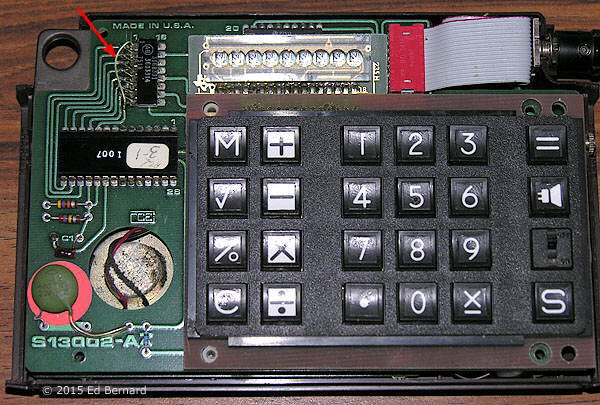
The Speech+ with the front cover removed. The red arrow points to a hand-wired modification required on this prototype circuit board.
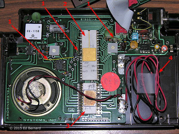
The Speech+ with the rear cover removed.
The red arrows are marked with different numbers which denote:
"1" - Hand-wired modifications required on this prototype circuit board.
"2" - TSI S14001A speech integrated circuit.
"3" - GI S14007 mask ROM integrated circuit with the speech data .
Note that initial prototype samples of the integrated circuits were supplied in the ceramic package seen here. Production parts were supplied in plastic packages, though both samples and production parts used the same silicon layouts.
"4": The batteries had started leaking so have been replaced by leads to connect to a laboratory power supply.
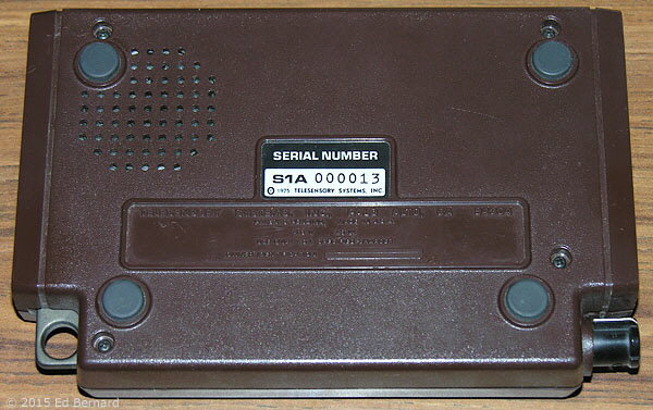
The rear, showing the serial number 000013.
These photographs can be compared with those of a production Speech+.
To play a .wav file supplied by Ed Bernard with the 24 sounds of the Speech+ click below (requires a soundcard and speakers)
Dale Hill has put a video of a Speech+ calculator in operation on YouTube, so that you are able to hear it in operation.
Ed Bernard continues:
"I had no involvement with the encoding of the speech. I don't know whether that was done by Dr. Mozer, TSi or both. Also I presume there was a TTL mock-up although it wasn't mentioned in my contacts with TSi.
The synthesis algorithm is pretty basic. I speculate that the generation of the data for this basic algorithm was where the real complexity lay (and I cannot help here in any way).
There is the concept of a "pitch period" which was is divided into 128 intervals. It represented one fluttering of the vocal cords and is the period of the fundamental frequency heard in say a long drawn out 'M'.
It's concept is used for both voiced (vocal cords fluttering - as in "my") and unvoiced (sibilants - as in "six") speech. Note there are also mixed phonemes as in the initial sound in 'Z'. There was no method for inflection (modification of the pitch period), thus the flat sounding synthesized speech. For a 10mS pitch period (100Hz) the output was updated every 12.8KHz. The nominal S14001A frequency was 13KHz.
Dr. Mozer's algorithm approximated voiced speech with the cords fluttering in the first half of the pitch period, and the second half quiet. I don't know how good an approximation this is, but it worked. This is factor of two savings for voiced phonemes.
As is applied today in MP3 compression the brain/ear system is not sensitive to relative phases of different frequencies, just to the frequency mix alone. Thus the frequencies in the first half of the pitch period were analyzed and the phase information removed. What this means in practice is that only the first quarter of the pitch period need be stored. The second quarter is just the first quarter played backwards. Another factor of two for voiced phonemes.
Non-voiced phonemes did not have this net factor of four savings.
The sound level was quantized in four bits, a far cry from MP3 quantization of 16 bits. But adequate for this application. Further the levels were not stored as four bits, but rather a 2 bit delta. A factor of two savings for both voiced and unvoiced speech. The two bit deltas were applied in an interesting fashion to the four bit sound level.
The initial sound level needs to be set at some time. I'm not sure whether is set to 0111 or 1000. My recollection is 1000. I'm vague as to when it was set. It would make sense, from a vocal cord point of view, to set it's initial value at the beginning of a voiced pitch period.
The direction of the last delta was remembered and used to modify the action of the current delta. At the beginning of a voiced pitched period the last direction was set to "up". I don't think it was forced at the beginning of a non-voiced pitch period. The last direction may have been set to "up" at the beginning of a control word (see below).
The two bit deltas were applied to the 4 bit sound level as follows (Action is the amount added or subtracted:
Delta Last Direction Action New Last Direction
00 Up
-1 Down
01
Up 0
Up
10 Up
+1 Up
11
Up +3 Up
00 Down
-3 Down
01
Down -1 Down
10 Down
0 Down
11
Down +1 Up
I believe this is the actual coding of the two bit deltas. Different assignments are certainly possible.
ROM Data Layout
This is to the best of my recollection. Many variants are possible. I have not yet looked at any reverse engineering information so as to not taint my recollection.
There is a potential ambiguity in the use of "word" below. "Word" will be used to refer to a spoken "word". Word will be used to refer to 16 bits of storage.
There are three types of storage.
- "Word" vector table
- Control words
- Delta bytes
The ROM consisted of 4K bytes. Thus a ROM address consisted of 12 bits, which were output from the S14001A in parallel. The calculator chip, which controlled the S14001, sent 6 bits of information as to which "word" was to be spoken. Thus the low 128 bytes of ROM were used to convert the 6 bit "word" into a 12 bit address of the first of many control words. Each vector consisted of two bytes. The low order 4 bits of the first byte were the 4 most significant bits of the resultant 12 bit address. The high order 4 bits were not used. The second byte was the low order 8 bits of the resultant address.
Control words consisted of two bytes. Each control word represented one or more pitch periods. The high order 4 bits of the first byte were control bits. The low order 4 bits were the 4 most significant bits of a 12 bit address of deltas for the control word. The second byte was the low order 8 bits of the delta address. The control bits were as follows from msb to lsb:
- voiced
- stop don't do any more control words. Wait for next "word".
- repeat count Two bits.
For voiced, this represented 1-4 repetitions of the same group of 8 delta bytes.
For unvoiced this meant output 1-4 pitch periods. 32 bytes for each pitch period.
I'm pretty sure this was 1-4 and not 0-3 as 0 would make no sense, but 5 would be an advantage.
Control words were consecutive in memory for a given "word" and could start on any byte address.
Delta data consisted of multiple bytes. For a voiced control word only
8 bytes were needed. (4 deltas per byte, thus 32 deltas total. Played forward for 1st quarter of pitch period, backward for second quarter, silence for last half.) Unvoiced required 32 bytes for each pitch period. Thus up to 160 bytes for 5 pitch periods ('S's were expensive, but the same deltas could be used by many different "words")! Deltas were consecutive in ROM and could start on any byte address.
Basic Overview of Operation of the S14001A
The calculator chip presented the "word" number on the 6 "word" lines and raised the start line. This could occur at any time during synthesis and would restart with the new "word". The word number was latched into the chip and used to fetch two bytes of control word address.
The two byte control word was accessed, the control bits stored in latches and the delta address latched.
The pitch period(s) determined by the control word were played.
If the stop bit was set the chip entered idle state, else the next control word was fetched and executed.
Laying Out the Design
The CAD involved was an in house graphics program for capturing layout information via a digitization tablet. This software performed basic layout rules checking and provided plots via a Versatec (wet xerographic process) computer printer. This all running on a 16-bit mini computer, an Interdata 7-16.
Basic logic pulldown to pullup ratios were determined using MOS models with SPICE verification. This was run on a Xerox Data Systems Sigma 7, time sharing from University of California, Irvine. The speed of operation of the device was slow enough that only one timing simulation was done to verify operation of the assumed critical delay path.
I wrote a simple logic simulator consisting of Fortran routines to verify logical operation. The chip contained 3 PLAs (Programmable by the chip designer) and these were also part of the simulation. This ran on the 16 bit mini.
Layout was done by hand in multiple small pieces, there was never a full layout of the entire chip But there was a full plot. The in house graphics information was converted to Calma GDS format and rubyliths were cut at a mask manufacturer in Costa Mesa.
As an aside, our Interdata 7-16 had a 9 track magnetic tape drive. Calma used 7 track. So we wrote a specially formatted 9 track tape, used a PDP 10 at UC Irvine to convert the tape to 7 track, which was then read by the Calma system.
What I referred to as the implant mask was what allowed the ion implant into the gate area of the depletion loads. P-Channel transistors are naturally enhancement mode (off when gate at source voltage), thus the p-implant to form depletion mode transistors. It was a metal gate process. The circuit design is much like n-channel but with voltages reversed.
From a logic standpoint I always worked assuming internal negative low voltages were logical true. There was an inversion at the inputs and outputs to turn internal negative low as true to external positive high as true. By keeping the conversion "at the door" the same schematic would work just a well for n-channel as for p-channel except for the "door" inversions.
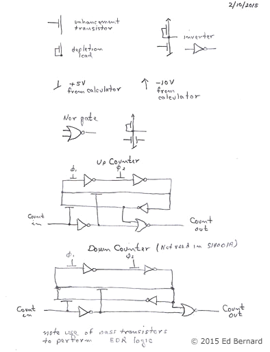
The attached document describes a virtual machine to implement the algorithm and ROM data description in my previous email. As I did that machine description and sketched out a counting register cell I came to realize I have probably gotten the ROM data layout wrong. This realization is driven by some detailed memories. And what follows may be incorrect in its details, as there are many variations that would accomplish the same thing. Regrettably I threw out my enlarged picture of the S14001A chip some years back as it would help pin down some uncertainties.
The modified ROM data layout
The first 128 bytes are pairs which vector the "word" number to the beginning control word for that "word".
The first byte contains the 8 most significant bits of the control word address. The second byte contains the 4 least significant bits of the control word address. I'm not saying where but an analysis of the ROM data might pin this down.
The first byte of the control word contains the 8 most significant of the delta data location. The second byte contains the next most significant bit (not bits), voiced, stop and 5 bits of repetition count. Since only 9 bits of address information is specified, zero is assumed for the low 3 bits of the address. Thus delta data must start on
8 byte boundaries. This wastes very little ROM since delta data always comes in multiples of 8 byte groups. It allows the repetition count to be up to 32 instead of four.
These changes simplify the virtual machine which I'll sketch out below.
The description below relies on the information in the document attached.
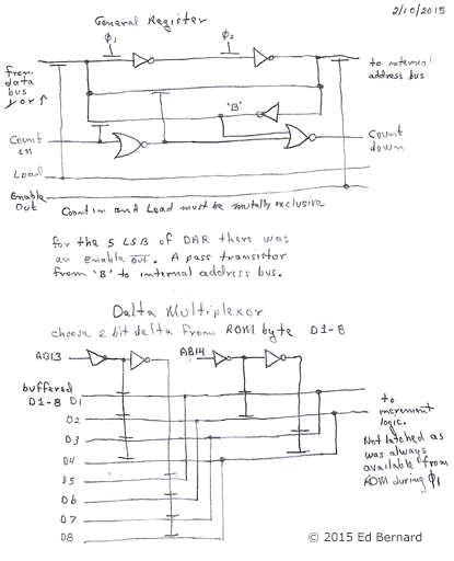
The data address register (DAR) no longer needs to count up 32 times, then down; it need only count up. Counting down is accomplished by inverting the 5 least significant bits of the DAR as they are applied to the ROM address and delta multiplexer (8 bits to two bits). The least two least significant bits of DAR (a 14 bit register) control which of the four deltas in a byte are used for the two bit delta. DAR now needs two increment controls, one for the 9 most significant bits and one for the 5 least significant bits.
The repetition register now becomes a 7 bit register which counts up.
The high order 5 bits come from the inverse of the 5 repetition bits in the second byte of the control word.. The low order two bits are forced to zero when the register loads. These two bits count the four 32 clock periods in a full 128 clock pitch period. The lsb of this register is given an alias name Down and the next lsb is aliased as Silent. This register is incremented when the 5 least significant bits of DAR carry.
There is no longer a pitch period register. It's function is replaced by the 5 least significant bits of DAR and the two least significant bits of the repetition register.
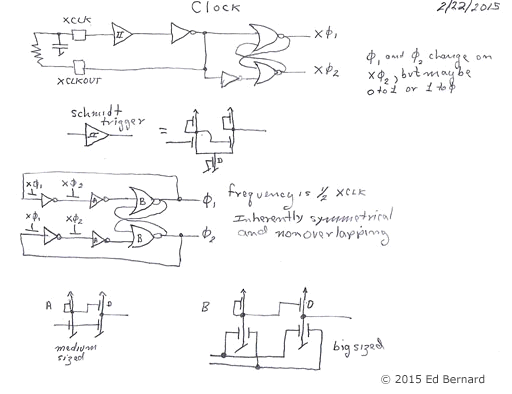
Enough of this. At least the general idea of the state machine has been conveyed. Some chip specific details and circuit examples are shown below." [Click on them to see larger versions.]
Jonathan Gevaryahu became fascinated by the ground-breaking speech synthesis in the Speech+ calculator and after initially finding great difficulty in obtaining information about the TSI S14001A managed use "reverse engineering" to determine a great deal about it. His findings are published in "TSI S14001A Speech Synthesizer LSI Integrated Circuit Guide" (referred to below as "JG's S14001A Guide") and in the the code in the links on Mameworld (referred to below as "Mameworld")
After reading "JG's S14001A Guide" and "Mameworld" Ed Bernard explained:
"I've now obtained and mostly read "JG's S14001A Guide" and "Mameworld". And I realize that my second reconstruction was not accurate either, but was headed in the right direction. Kudos to Jonathan Gevaryahu and Kevin Horton (G&H) for teasing out so much information. I'll defer to G&H's definition of the ROM data, their delta table, and the extra bit in both the repeat count and length, and the pinout. I am assuming Jonathan 's software works and produces proper speech, at least for some games. I have looked through the code and it appears it would work.
A couple of observations:
In both the "JG's S14001A Guide", and the source code it is mentioned that there is no way to stop the S14001A from speaking. This is technically not correct. While
the chip has no overriding reset, Start will interrupt any state and force the next state to start a new word. Thus simply by speaking the shortest silent word, the chip could enter it's idle state within 20mS. The
Speech+ used the programmable calculators power on reset and the calculator caused the Speech+ to say "clear" on power up, thus putting the S14001A in a known state. There is no indication of this
"Start" activity in Jonathan's code, which should have an if test in each state to force the next state to one if Start is asserted. This feature also made testing easy as the internal chip state could easily be
forced by the test equipment asserting Start.
State 13 of Jonathan 's code provides a delay of two external clocks. I presume this delay was to match the delay in the chip's digital to analog converter. The analog output would be one internal clock later than the digital output. So technically the chip would be busy for an additional internal clock.
There is no filter in the S14001A. It's analog output consisted of 16 levels with clock noise superimposed. The output never floated, but was driven by a source follower. Any analog filtering, and there was some was done external to the chip. I did hear the TSI project leader mention a "brick wall" filter.
In "JG's S14001A Guide" Jonathan Gevaryahu mentions Dr. Mozer's sons and a company called SSI. There was no contact between Dr. Mozer or his sons and Silicon Systems, Inc. also known as SSi.
I've attached some schematics for typical circuitry in the S14001A (poorly hand drawn). Note that the chips internal clock was a division by two of the external clock. Further, on power up, the internal clock could come up in either state, so when testing the chip, Pin 9 - "Address Read", had to be watched for two external clocks to synchronize the test equipment to the chips internal clock state.
One important aspect of the forward/reverse playing in the first/second quarters of a pitch period is that they were exact mirror images. That is, the output values for internal clocks 00-31 and 32-63 were identical. (32=31, 33=30, ...63=00). To make this happen no increment must be applied at clock 32. Jonathon's comment in reveng.pdf: "If we're immediately after the mirror point in a mirrored sample, the last accumulator output is simply repeated and not recalculated using the delta. The old/new deltas update as usual though. **this is very important!** And from the source code: "if (m_laststate != 8) // ignore first (bogus) dac change in mirrored backwards mode. observations and the patent show this"."
© Ed Bernard & Grant Still Shatto, II 2015.
Sources:
- Hill, Dale, Speech+ calculator in operation on YouTube at https://www.youtube.com/watch?v=Slyet_K87oQ.
- Bernard, Ed., "Speech+ State Machine".
- Gevaryahu, Jonathan, "TSI S14001A Speech Synthesizer LSI Integrated Circuit Guide" at https://archive.org/stream/pdfy-QPCSwTWiFz1u9WU_/david_djvu.txt.
- Gevaryahu, Jonathan, "S14001a plus SND-1000 code" at http://www.mameworld.info/ubbthreads/showflat.php?Cat=&Number=90528&page=0&view=expanded&sb=6&o=&vc=1.
- A link for information about Silicon Systems, Inc. is http://en.wikipedia.org/wiki/Silicon_Systems.
Calculator Articles
Vintage Calculators
Text & photographs copyright, except where stated otherwise, © Nigel Tout 2000-2026.
